Research
We measure the mechanical properties of molecular semiconductors on the nanoscale.
Why does this matter? The materials behind flexible displays, wearable sensors, and printed solar cells are soft, disordered, and only nanometres thick — and how stiff or pliable they are at that scale governs how well they work and how long they last. By measuring mechanics on the molecular level, we connect a material’s physical structure to the way it carries charge and heat, which helps in designing better devices.
Techniques
We implement cutting-edge force mapping using atomic force microscopes, based on multifrequency intermodulation, higher eigenmodes, and quasi-static nanoindentation. We have visualised high-contrast elasticity at the scale of a few nanometres [see Nature Communications 13, 3076 (2022)] and resolved the elastic contribution of individual molecules within a molecular lattice [see Nature Communications 17, 1621 (2026)]. Current projects track how elasticity evolves through temperature-induced and cooperative phase transitions, at reduced dimensions, at the limits of charge conduction, and within prototype microfabricated devices.
The underlying physics
Macroscopic stiffness is the long-wavelength, zero-frequency limit of the acoustic phonon response. Macroscopic stiffness is thus not a concept separate from phonons. It is what phonons become in the limit.
At a fundamental level, we are interested in how carrier mobility, electrical conductivity, the Seebeck coefficient, and elasticity interlock within a single multifunctional material — treating mechanics not as a separate engineering concern but as one face of the same underlying physics that sets electronic and thermal transport. One framework we have proposed is summarised in the schematic below.
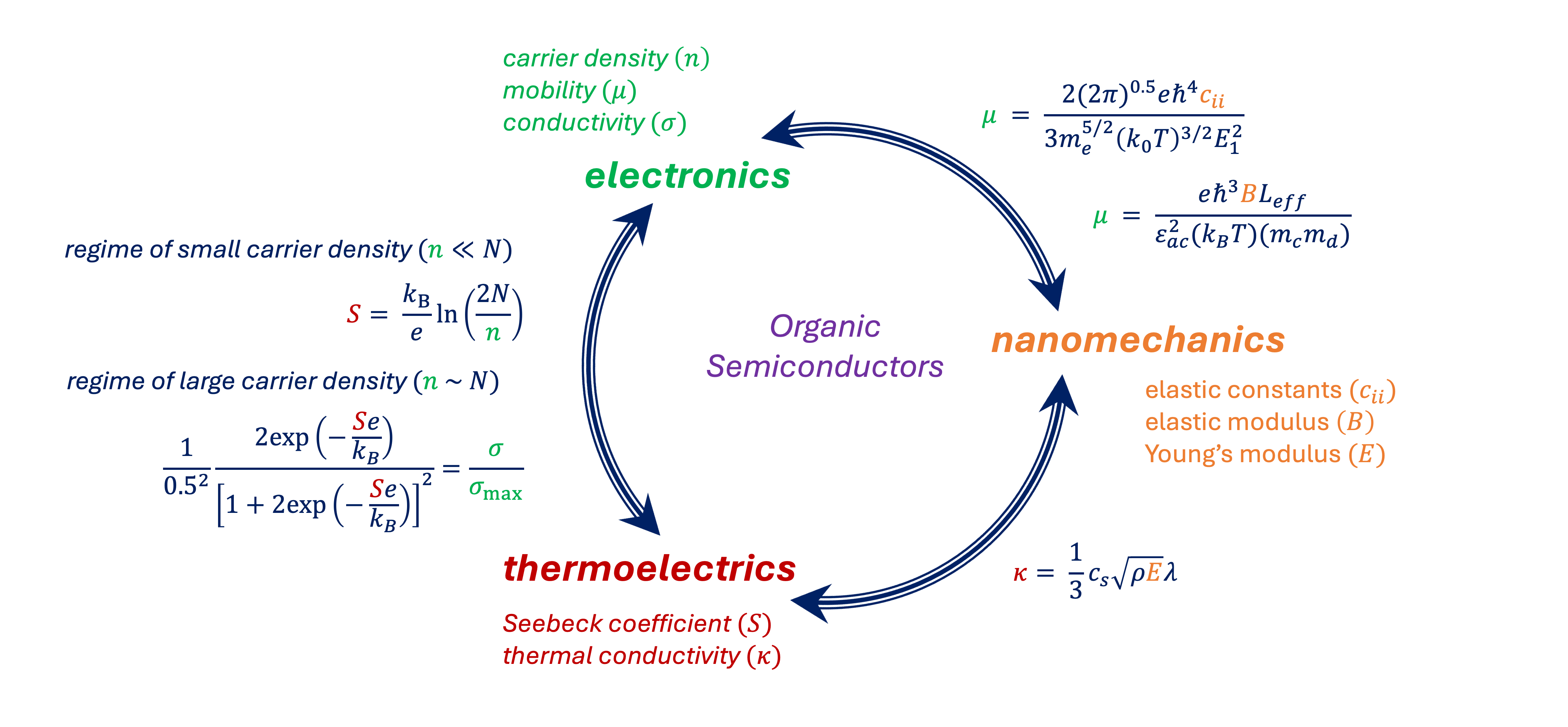
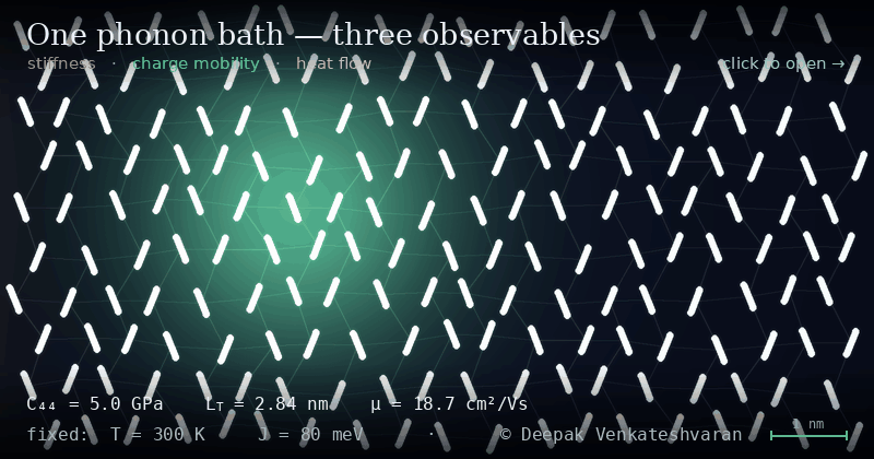
The mechanistic flow that connects the shear modulus with its charge carrier mobility arises when combining the shear elastic constant c44 with transient localisation theory. Click the interactive illustration below to see how such a mechanism plays out. The sliders can be used to tune the shear modulus of an organic molecular semiconductor and look at its impact on the mobility. This interactive plot is phenomenologically correct, but does not include quantum corrections to displacements at very low temperatures.
Collaborations
I run the core program with Dr Ki-Hwan Hwang and Mr Mateo Cervantes in Cambridge, and with Prof Per Claesson in Stockholm. Strong industry ties come through our partnership with Park Systems. For the theory and calculation of molecular mechanics, I work with Prof Erin Johnson and Prof Yoann Olivier.
Beyond electronically active materials, we work closely with Prof Ljiljana Fruk and Dr Leszek J. Spalek to extend our methods to biological and biocompatible matter.
Since 2024, I have jointly run a program on molecular thermoelectrics with Dr Guillaume Schweicher at ULB in Belgium and Prof Kazuo Takimiya at RIKEN in Japan, seed-funded by the Wiener Anspach Foundation.
Funding
The program is supported by multiple research grants from the Royal Society, for which I am deeply grateful.